This document presents thermal modeling results of a monolithic half-bridge GaN power integrated circuit (IC) with integrated gate drivers, focusing on its thermal behavior and electrical characteristics.
Thermal Simulation and Key Findings
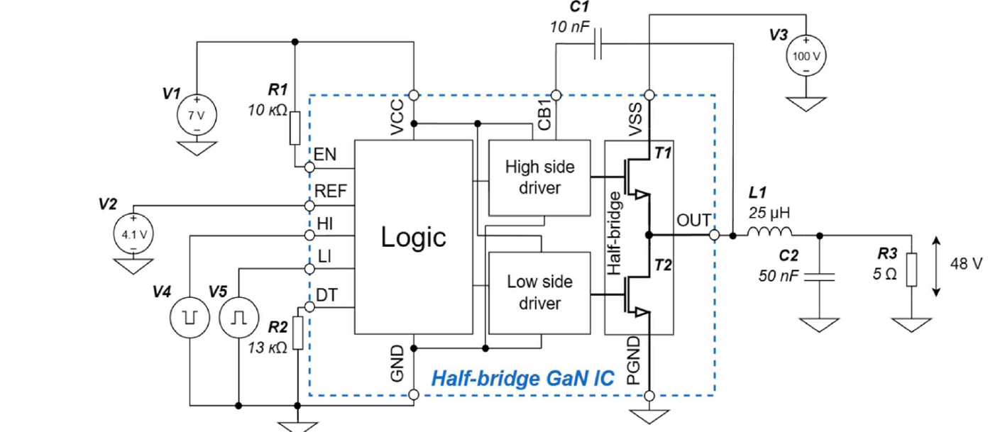
The study evaluates the thermal performance of a GaN half-bridge IC developed on the IMEC GaN-on-SOI platform, particularly in a buck synchronous DC-DC converter application.
The primary heat sources identified are the half-bridge GaN high-electron-mobility transistors (HEMTs), which significantly influence the temperature of adjacent components, including logic blocks and gate drivers.
Increased temperatures in the IC lead to higher channel resistance in the HEMTs, resulting in reduced output current and increased switching times for the drivers, ultimately degrading the dynamic performance of the IC.
Introduction to GaN Technology
-
Gallium nitride (GaN) is recognized for its superior properties over silicon, including a wide bandgap, high critical electric field, and enhanced carrier mobility, making it suitable for high-efficiency power electronics.
GaN devices exhibit low on-state resistance and high switching speeds, but their compact size leads to increased heat generation, necessitating advanced thermal management strategies.
Despite their advantages, GaN power ICs face challenges such as the need for complementary logic transistors and effective heat dissipation methods to ensure reliability.
Methodology
-
The investigation involved two stages: first, assessing the average power dissipated in the functional blocks of the GaN half-bridge IC; second, evaluating how die temperature affects the electrical characteristics of these blocks.
Simulations were conducted using Cadence Virtuoso with verified e-mode GaN HEMT models, focusing on a DC-DC converter configuration.
Results of Power Dissipation Analysis
-
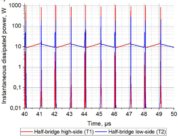
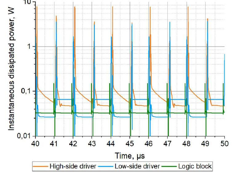
The average power dissipation was calculated for the high-side and low-side HEMTs, drivers, and logic block, revealing that the high-side HEMT dissipated 11.8 W, while the low-side HEMT dissipated 9.15 W.
The total power loss in the GaN half-bridge IC was found to be 21.2 W, with an overall efficiency of approximately 96% based on an input power of 530.5 W.
Impact of Die Temperature on Electrical Characteristics
-
The study found that increasing the die temperature from 25 °C to 150 °C resulted in:
An increase in channel resistance of the half-bridge HEMTs from 0.1 Ω to 0.15 Ω, leading to a drop in output current from 16 A to 10 A.
A reduction in driving current for the high-side and low-side drivers from 500 mA to 270 mA, which increased the switching times significantly.
A doubling of the rise time of output signals from the logic block, extending the duration of transient processes during switching.
Conclusion and Future Work
-
The thermal simulation results indicate that the heating of the GaN half-bridge IC adversely affects its electrical performance, particularly through increased channel resistance and switching times.
The findings underscore the need for optimized IC layouts and effective heat transfer solutions to mitigate thermal issues and enhance reliability.
Future work will focus on refining the design of GaN IC functional blocks to improve thermal management and overall performance.
Acknowledgments
-
The research was funded by the Federal State Budgetary Institution and acknowledges support from the Center for Collective Design of Electronic Components and Radioelectronic Equipment at MIET, as well as contributions from colleagues in the field.
This summary encapsulates the essential findings and methodologies of the thermal modeling study, highlighting the implications of temperature on the performance of GaN power ICs.
Figures
Fig. 1. Schematics of synchronous buck DC-DC converter used for investigation of average power dissipated in functional blocks of GaN half-bridge IC.
Fig. 2. Time dependences of the instantaneous power dissipated in the half-bridge (a), in high- and low-side drivers, in logic block (b).