This document investigates the influence of heterostructure parameters on the performance of microwave transistors, specifically focusing on high electron mobility transistors (HEMT).
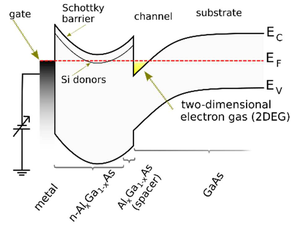
Fig. 1. Band diagram of HEMT heterostructure
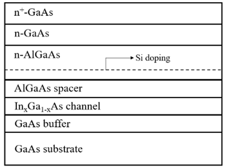
Fig. 2. Cross section of pHEMT heterostructure.
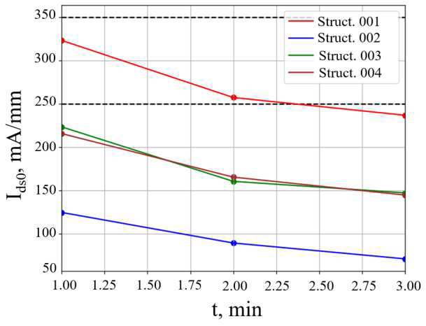
Fig. 3. Calculation results of the drain current per unit width of the channel at a gate voltage of 0 V at different etching times of the gate recess.
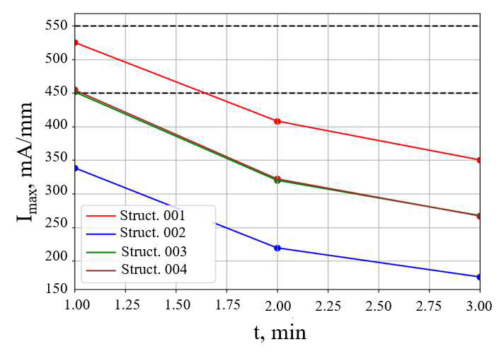
Fig. 4. Calculation results of the maximum drain current per unit channel width at different etching times of the gate recess.
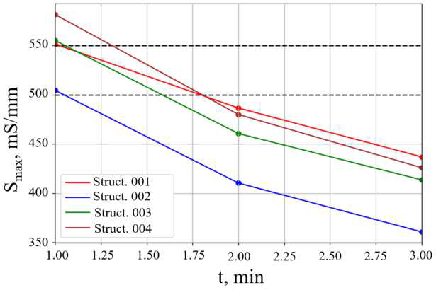
Fig. 5. Calculation results of the maximum value of transistor steepness per unit width of the channel at different etching time of the gate recess.
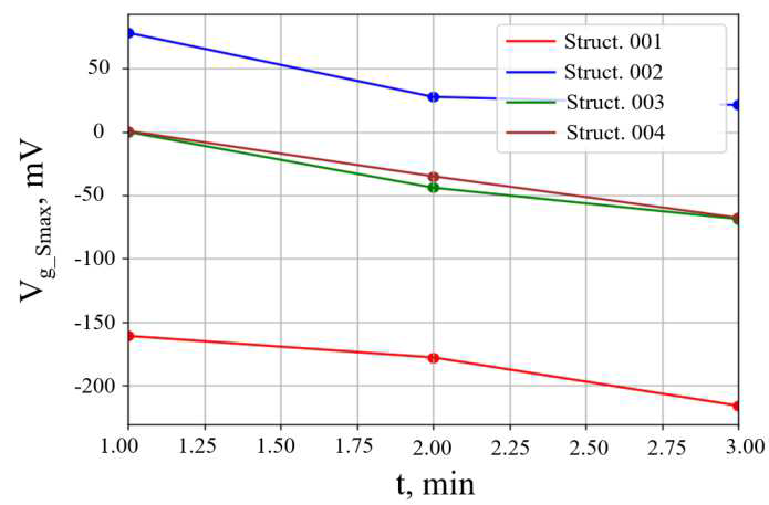
Fig. 6. Calculation results of the position of the maximum steepness of the transistor at different etching times of the gate recess.
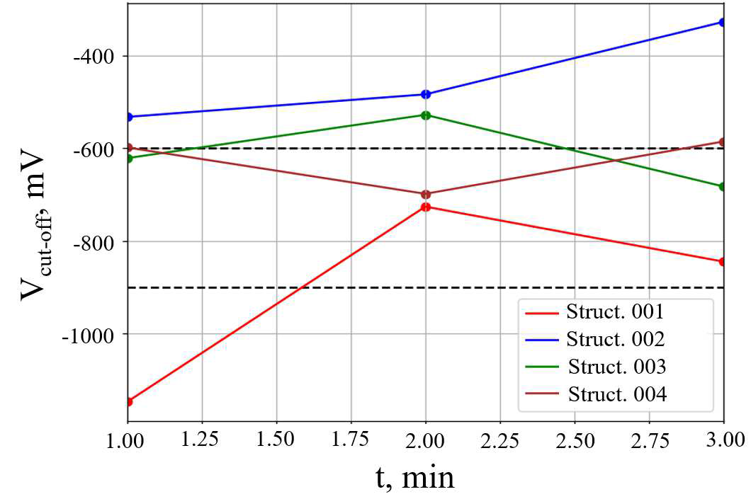
Fig. 7. Calculation results of the transistor cutoff voltage at different etching times of the gate recess
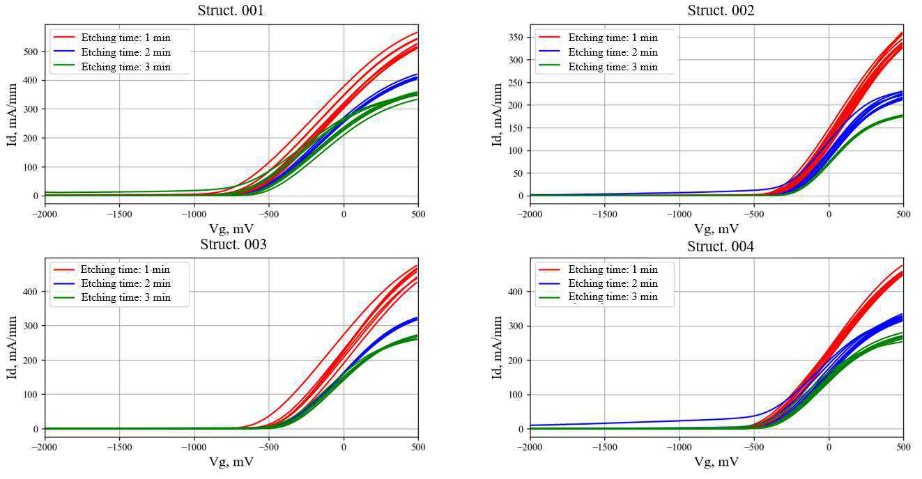
Fig. 8. Dependence of the drain current on the gate voltage at different etching times of the gate recess.
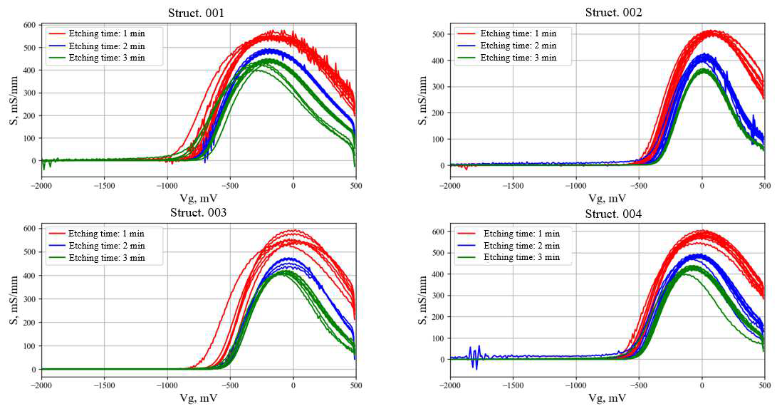
Fig. 9. Dependence of the transistor steepness on the gate voltage at different etching times of the gate recess.
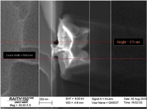
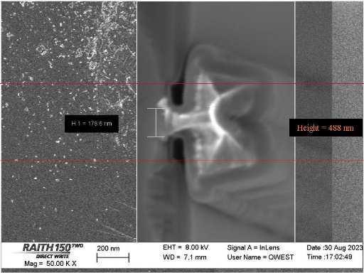
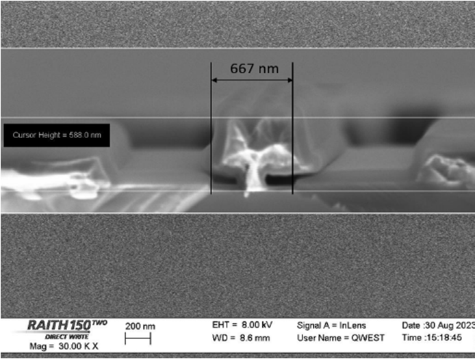
Fig. 10. SEM images of etching profiles of the gate recess for all values of etching time: (a) 1 min; (b) 2 min; (c) 3 min
Heterostructure Selection and Experimentation
-
The study analyzes four different heterostructures fabricated using 0.15 μm pHEMT technology, each varying in carrier mobility and doping concentration.
Key parameters measured include drain current per unit channel length at zero gate voltage, maximum drain current, cutoff voltage, and maximum steepness of the transistor.
The optimal heterostructure was identified as Struct. 004, which exhibited a carrier mobility of 5005 cm²/(V·s) and a doping concentration of 1.31·10¹² cm⁻².
Gate Recess Etching Optimization
-
The research also aimed to determine the optimal etching time for the gate recess, tested at 1, 2, and 3 minutes.
Results indicated that the best etching time for achieving desired transistor characteristics is approximately 1.5 minutes, balancing breakdown voltage and transistor performance.
Experimental Results and Analysis
-
Transfer characteristics were measured at a drain-to-source voltage of 1.5 V, revealing variations in transistor performance based on heterostructure and etching time.
Breakdown voltages increased with longer etching times, with values of 6-7 V for 1 min, 12 V for 2 min, and 15 V for 3 min.
However, longer etching times negatively impacted transistor characteristics, such as maximum steepness and drain current at zero gate voltage.
Conclusions and Implications
-
Struct. 001 was determined to be the most effective heterostructure, achieving superior drain current and steepness due to its higher carrier concentration.
The study concludes that while increased etching time enhances breakdown voltage, it also deteriorates other critical transistor parameters, emphasizing the need for careful optimization in the fabrication process.
The proposed approach for selecting optimal heterostructures involves iterative testing and evaluation of electrical characteristics to refine parameters for achieving desired MMIC performance.
Acknowledgments
-
The research was supported by the Ministry of Science and Higher Education of the Russian Federation and conducted by the Integrated Optics and Radiophotonics Laboratory at Tomsk State University of Control Systems and Radioelectronics.
This summary encapsulates the essential findings and methodologies of the study, highlighting the significance of heterostructure design and etching processes in optimizing microwave transistor performance.
Tables
| HETEROSTRUCTURE PARAMETERS | ||
|---|---|---|
| Heterostructure Designation | Carrier Mobility in the Channel, cm2/(V·s) | Concentration of Carriers in the Channel, cm-2 |
| Struct. 001 | 4391 | 2,19·10^12 |
| Struct. 002 | 4832 | 2,00·10^12 |
| Struct. 003 | 5280 | 1,24·10^12 |
| Struct. 004 | 5005 | 1,31·10^12 |
| TRANSISTOR PARAMETERS | ||
|---|---|---|
| Parameter | Description | Target Values |
| Ids0 | Drain current per unit channel width at gate voltage Vg = 0 V | (250…350) mA/mm |
| Imax | Maximum drain current per unit channel width | (450…550) mA/mm |
| Vcut-of | Transistor cutoff voltage (determined at Id = 1 mA/mm) | (-600…-900) mV |
| Smax | Maximum transistor steepness | (500…550) mS/mm |
Figures
Fig. 1. Band diagram of HEMT heterostructure
Fig. 2. Cross section of pHEMT heterostructure.
Fig. 3. Calculation results of the drain current per unit width of the channel at a gate voltage of 0 V at different etching times of the gate recess.
Fig. 4. Calculation results of the maximum drain current per unit channel width at different etching times of the gate recess.
Fig. 5. Calculation results of the maximum value of transistor steepness per unit width of the channel at different etching time of the gate recess.
Fig. 6. Calculation results of the position of the maximum steepness of the transistor at different etching times of the gate recess.
Fig. 7. Calculation results of the transistor cutoff voltage at different etching times of the gate recess
Fig. 8. Dependence of the drain current on the gate voltage at different etching times of the gate recess.
Fig. 9. Dependence of the transistor steepness on the gate voltage at different etching times of the gate recess.